Build a Roamyboard

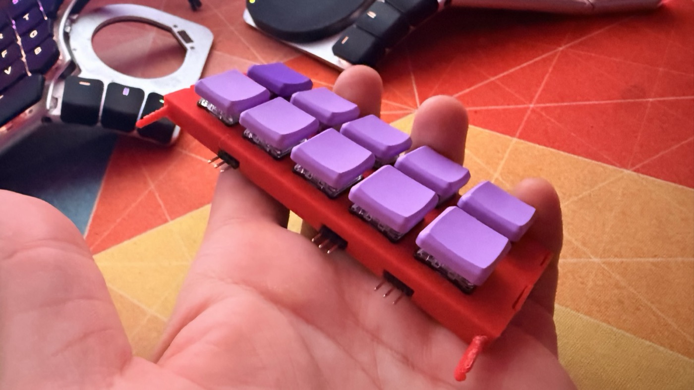
A keyboard you wear on your leg, made of printed modules that click together side by side. Each key module carries one column of five keys; add or remove them while it runs.

8°between neighbouring modules, so a half curves around the leg
5Choc keys per key module, hot-swappable
anynumber of key modules per half; the firmware counts them

Plan your build → What's in a half

A project by Nevyn Bengtsson, 2025–2026.

Drag to orbit, scroll to zoom, and drag the slider to add key modules. Every 3D view in this guide is generated from the same Cadova model that the parts print from.

1

What you're building

A half is a row of modules: a terminator module at the left end, any number of key modules, and the MCU module at the right end with the nice!nano, battery and display. A unibody keyboard is one half; a split keyboard is two.

Orientation

The modules of a half

#

Every module has two long sides, named by the connector on them:

  • The header side carries three headers (male, pins out) and the two guide pins. Headers face right, toward the MCU module.
  • The socket side carries three sockets (female) and the two guide holes with their flaps.

The terminator module has a header side only, and the MCU module a socket side only, so no header pins stand exposed at either end. Their other long side is the free face, which carries the lugs for the harness.

The two ends of a module are the SW1 end and the SW5 end, named by the switch nearest each. SW1 is the bottom key.

This guide uses the terms in docs/glossary.md. Hover a part in any 3D view to see its name.
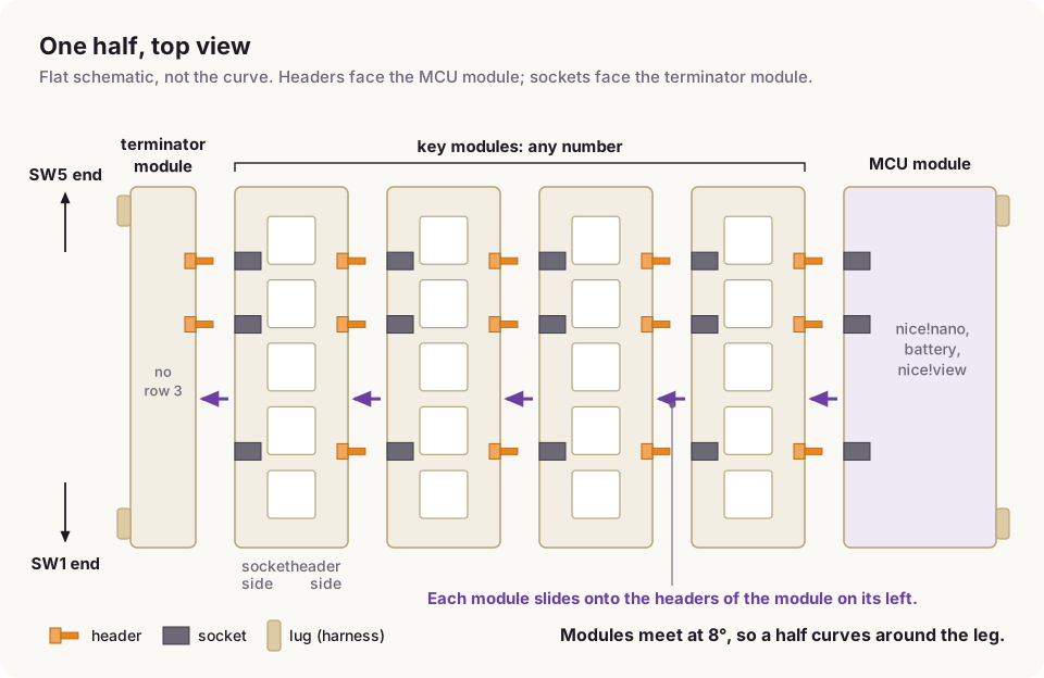
Top view of a half: terminator module, key modules and MCU module, with header and socket sides marked
Orientation

Parts of the joint

#

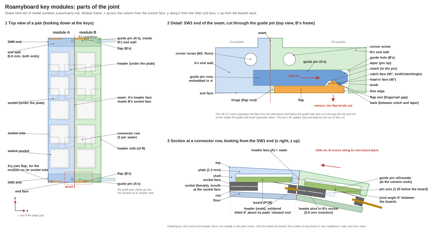
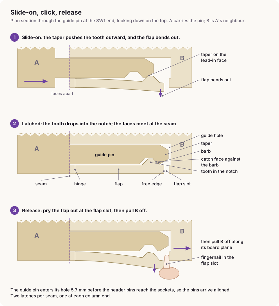
Neighbours couple at a joint: the header pins go into the neighbour's sockets, the guide pins into its guide holes, and a tooth on each flap clicks into a notch in the guide pin. The guide pins arrive first, so the header pins reach the sockets already aligned.

Labelled drawing of the joint between two key modules
From the glossary. Click to enlarge.
Electronics

How a half reads its keys

#

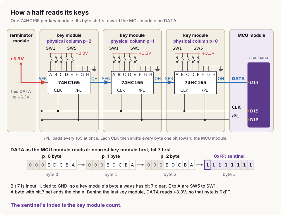
Each key module has one 74HC165 shift register. The registers of a half form the chain: every scan, the MCU module loads all of them at once and clocks their bytes out on DATA, nearest key module first.

The terminator module ties the far end of DATA to +3.3V, so after the last key module the chain reads 0xFF, the sentinel. A real key module's byte always has bit 7 clear, so the first byte with bit 7 set ends the chain, and its index is the key module count.

That is why modules can be added and removed while the keyboard runs, and why a half without its terminator module types nothing.

More in docs/firmware.md and electronics/Electronics.md.

The shift register chain of a half, and the bytes the MCU module reads
2

Plan and gather parts

Pick a layout and a key module count; the parts list and the print list below follow. The choice lives in the page's address, so a link to it keeps your plan.

Plan

Your build

#
7

The default keymap uses 7 key modules per half on a split and 14 on a unibody; see the keyboard layout. More key modules work; their keys map to &none until the layout grows.

Parts list

Tick what you have. Quantities follow the plan; order a few spares of the small parts.

PartSourceQty
Plan

Tools and consumables

#

Printing

  • A 3D printer, and a slicer that can paint supports and pause at a height
  • Filament: PLA or PETG. Which one holds the latch flap better is not tested yet.
  • Flush cutters and a deburring blade for the support under the guide pins

Soldering

  • Fine-tip soldering iron, thin solder and flux
  • Tweezers for the 0805 parts and the SOIC-16
  • Multimeter with continuity and DC volts
  • Thin hookup wire for the MCU module; insulated wire up to 1.3 mm across for the terminator module

Assembly

  • Two-component epoxy for gluing the connectors to the board; superglue if you have nothing else
  • A small Phillips driver for M2 screws
  • A USB-C cable for flashing and charging
  • A strap for the harness: the lug slots take up to 24 × 4 mm
3

Print the parts

The print files come from the Cadova model in case/roamy-v4. Each part carries its revision engraved (r6 and so on).

Files

Generate and check the print files

#
  1. In case/roamy-v4, run swift run. It writes build/roamy-v4/*.3mf and prints, among other things, the terminator module's pause height.
  2. Run python3 tools/check.py. It compares the board against KiCad's own 3D export (a mirrored model fails it) and checks the fits, the slide-on and the floors. Run it before printing anything.
  3. Run python3 tools/overhang.py. It slices the print poses at 0.2 mm and fails on anything that droops outside the painted-support zone.

Current revisions

PartFileRev
Key module shellkey-module-print.3mf
Key module floorkey-module-print.3mf
MCU shellmcu-module-print.3mf
MCU floormcu-module-print.3mf
Terminator moduleterminator-print.3mf
Solder jigsolder-jig-print.3mf

Read from Parameters.swift when the guide's models were generated.

Print

Print the solder jig

#

The jig holds a key module board front down and puts every connector where the case expects it: sockets against a stop at the mouth, headers tilted 8° in a cradle. One jig does every board.

  1. Print solder-jig-print.3mf, base down. It has no overhangs.
  2. The engraving on top reads 8° jig and its revision.
Print ×

Print the key module shells and floors

#
  1. Open key-module-print.3mf: the shell on its top, the floor beside it.
  2. Paint support under the two guide pins only (red in the view). Their lowest ridge is an 11 mm cantilever over the bed.
  3. Print of each.
  4. Remove the support from the guide pins and clean their ridges: they align the whole joint.

In the print pose, each switch seat hangs 0.57 mm over the empty pocket. The 0.4 mm chamfer on the opening's edge keeps that short enough to print as a slowed overhang wall. Whether it prints clean on every printer is not tested yet; stray strands in the openings can be trimmed.

Print ×

Print the MCU module

#
  1. Open mcu-module-print.3mf: the shell on its top, the floor beside it.
  2. No painted support: the MCU module has no guide pins. Its lugs print standing on the bed.
  3. Print of each.

The terminator module prints with a pause for its embedded headers, so it has its own chapter.

4

Solder the key module boards

Repeat for each key module board, and once more for the MCU module's socket board, which takes the sockets only (chapter 7). The board's front carries the passives and the switches; its back carries U1, the hotswap sockets and the connectors.

Front

Front: resistors and capacitor

#
  • R1 to R5: 10 kΩ, 0805. The pull-downs of the five keys.
  • C1: 100 nF, 0805. Decoupling for U1.

Do the front first: the jig holds the board front down, in pockets with room for these parts and their fillets.

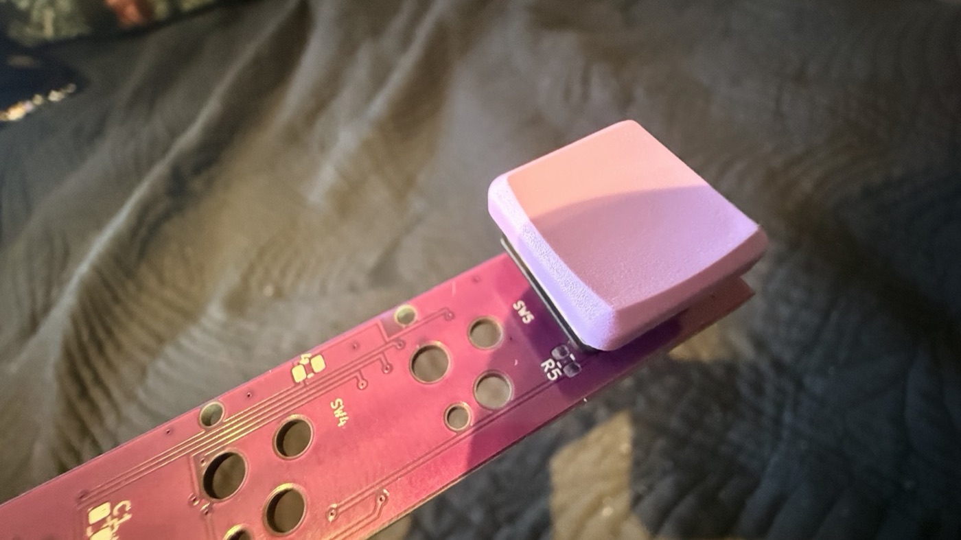
A bare purple key module board with one switch and keycap in the SW5 position
A bare v5 board's front, with a switch and keycap dropped into SW5 before anything was soldered (2026-09-23).
Back · jig

Back: U1, hotswap sockets and connectors, in the jig

#
  1. Lay the board front down in the jig's pocket: the SW5 and SW1 engravings mark the matching ends, and the header side faces the labels.
  2. Solder U1 (74HC165, SOIC-16). Mind pin 1.
  3. Solder the five Choc hotswap sockets, one above each key.
  4. Sockets (J_LEFT1 to J_LEFT3, socket side): each body rests on the board in its nest. Push it against the stop at its mouth, which sits 2.0 mm past the board edge, and tack one pad. Check, then solder the rest.
  5. Headers (J_RIGHT1 to J_RIGHT3, header side): see the next step.

Use the numbered buttons under the view to go through it.

Every cut in the jig is open toward the component side, so the soldered board lifts straight out.

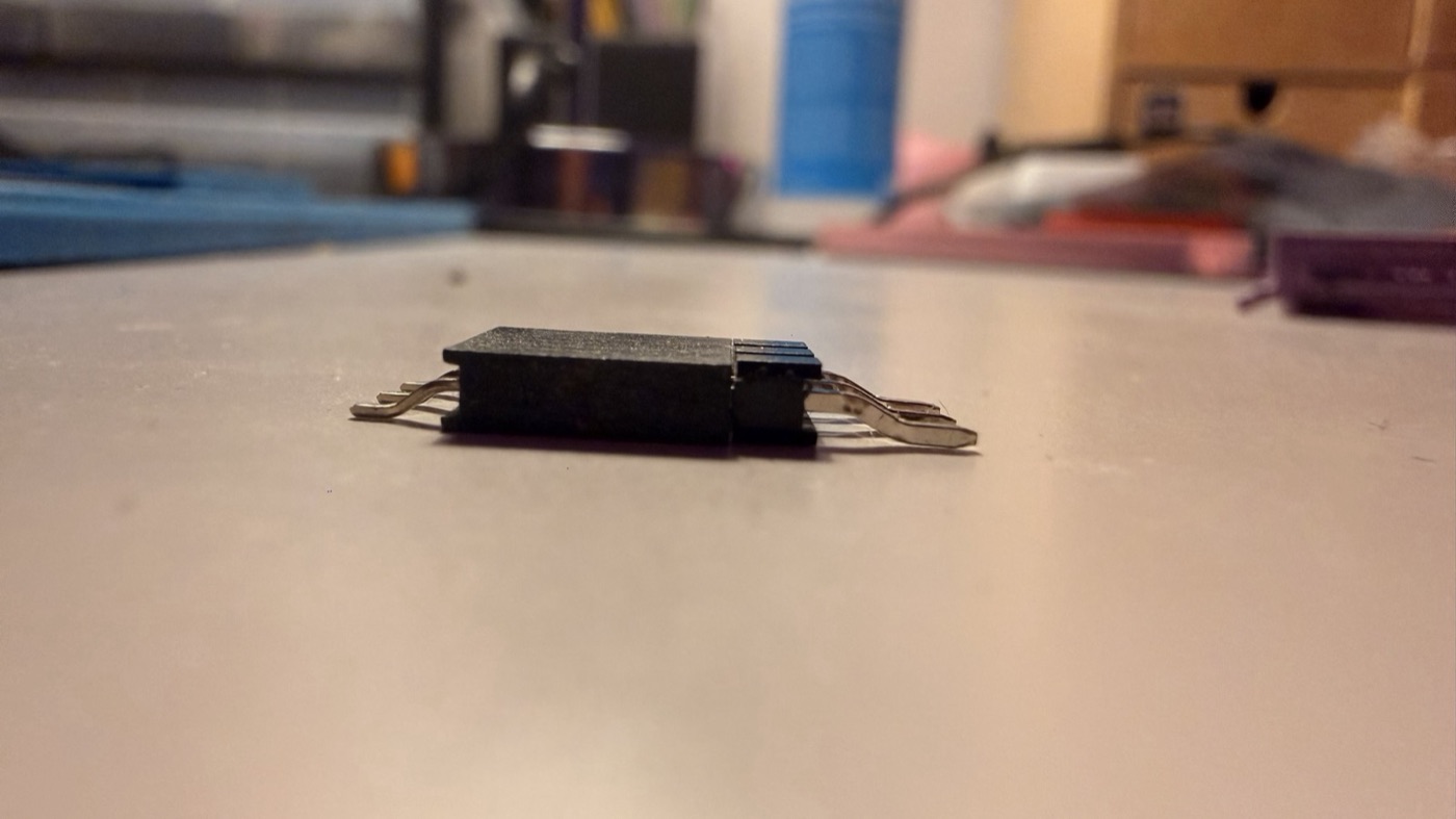
A header and a socket plugged together, lying on a table
A header and a socket, mated: both bodies rest on their feet, so a pair lies flat on the table (2026-09-25).
Back · jig

Headers at 8°

#

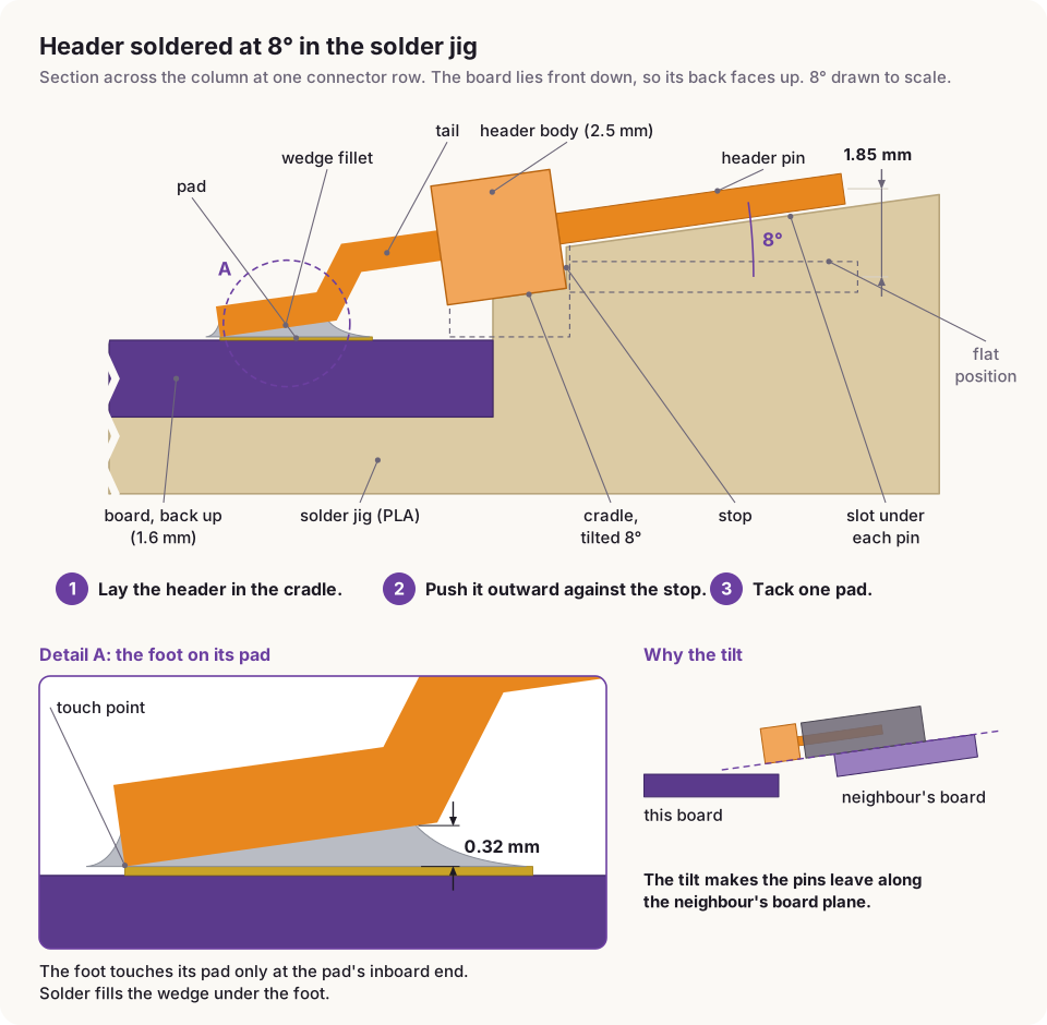
Neighbouring modules meet at 8°, so the header pins must leave along the neighbour's board plane. Instead of bending the pins, you solder the whole header tilted.

  1. Lay the header in the jig's cradle, which is tilted 8° about the inboard end of the pads, with a pin in each slot.
  2. Push it outward against the stop that touches the body's outer edge, and tack one pad.
  3. Solder all three feet. The foot touches its pad at the inboard end and has 0.32 mm under its other end, so each joint is a wedge-shaped fillet.

The wedge fillet must not carry the connector's load. In the case, the floor's rear stop takes the slide-on push and its clamp pad keeps the body from tipping; the glue, next, takes the pull when modules come apart.

Cross-section of a header soldered at 8 degrees in the jig
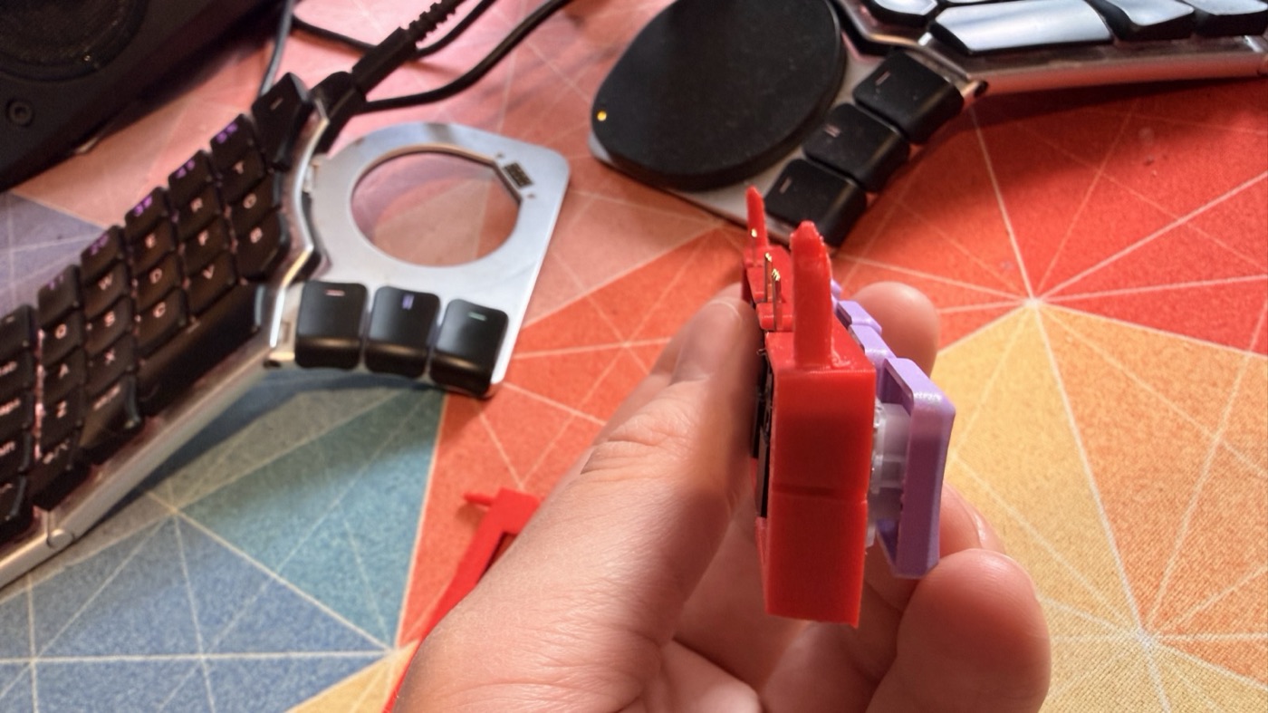
End view of a key module with the header pins and a guide pin sticking out
End view of a key module with headers soldered in the jig: the header pins run parallel to the guide pin (2026-09-26, an earlier case revision).
Back

Glue the connectors to the board

#

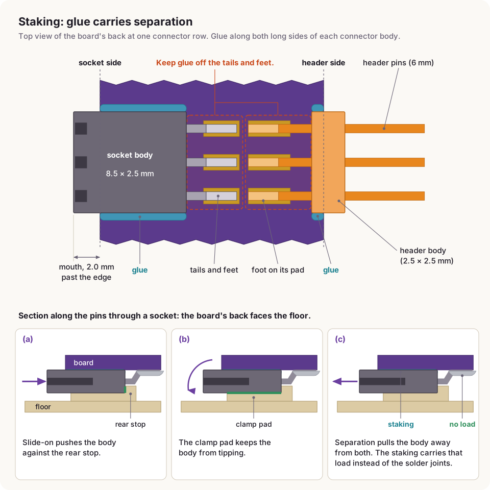
Glue the headers and sockets to the board, so that pulling modules apart pulls on the board and the case rather than on the weak solder joints. Nothing else can take that pull: at the seam, the header body and the neighbour's socket mouth are only 0.39 mm apart, which leaves no room for a stop. The glossary calls this staking.

  1. Mix a small amount of two-component epoxy. Superglue works as a fallback if you have nothing else.
  2. Run a bead along both long sides of each connector body, between the body and the board. Six bodies per board.
  3. Keep the glue off the tails and their fillets, and within about 0.5 mm of the body: the floor's clamp pads and rear stops need the rest.
  4. Let it cure fully before the board goes into its shell.
Where the glue goes along each connector body
Photo wantedA staked board: glue beads along a socket and a header.
Test

Optional: test the board on its own

#

firmware/shiftregister-test is an Arduino sketch for an M5StickC Plus that clocks the 74HC165 and shows every key on its screen. It needs the board's header pins and five wires:

M5StickC PlusKey moduleSignal
3V3J_RIGHT1 pin 2+3.3V
GNDJ_RIGHT1 pin 3GND
GPIO25J_RIGHT2 pin 1CLK
GPIO0J_RIGHT2 pin 2/PL
GPIO26J_RIGHT2 pin 3DATA (QH)

Tie J_LEFT2 pin 3 (DATA in) to GND for the test, so the bits shifted in behind the module read 0. Details in the sketch's README. Without an M5Stick, test the boards in the finished half instead (chapter 9).

5

Assemble the key modules

Board into the upturned shell, floor on, switches in. Repeat times.

Assemble

Board into the shell, floor on

#
  1. Turn the shell upside down. The revision is engraved on the SW1 end wall's inner face.
  2. Drop the board in along its normal, back up, SW1 at the SW1 end. The connectors go into the wall slots, which are open toward the floor. The ledges under the plate stop the board from rising further.
  3. Put the floor on. Its locating tabs find the shell's opening; the clamp pads land on the connector bodies and the rear stops behind them.
  4. Fasten it with four M2 × 5 mm self-tapping screws in the end walls' corners. The floor is 0.5 mm thick under each screw head and the pilots are 5 mm deep.

If the floor will not sit flat, look for a solder fillet or a glue bead in the way before you tighten the screws. The tightest spot is under the tilted header bodies.

Assemble

Switches and keycaps

#
  1. Turn the module right side up. Press a Choc v1 switch into each switch pocket until its side clips catch under the plate; its legs go through the board into the hotswap sockets.
  2. Put the keycaps on.

The switches are hot-swappable: pull one out with a switch puller to change it. The sockets hold the switch; the plate's 0.25 mm seat and the clips keep it square. How well the seat holds under hard typing is still to be tested.

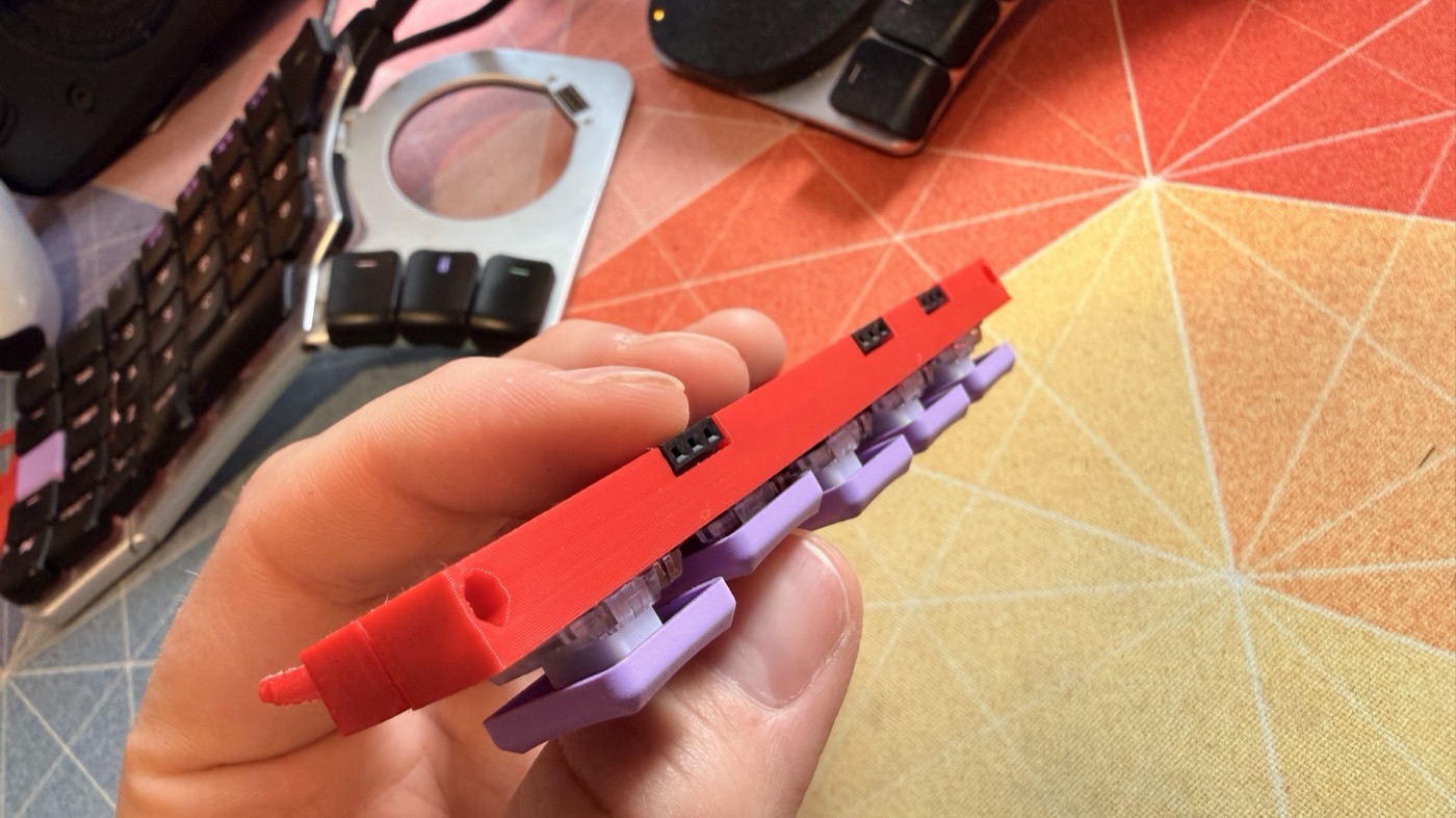
A finished key module held in a hand, with connector openings along its side
A finished key module (2026-09-26, an earlier case revision).
6

Build the terminator module

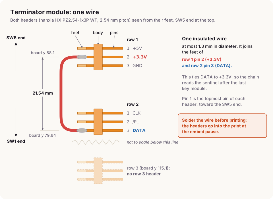
A solid print about 12 mm wide with two headers glued inside it, embedded during a pause in the print. Electrically it only ties its neighbour's DATA to +3.3V, which makes the chain end in the sentinel.

Solder

Solder the wire

#

Two headers sit where a key module's would: row 1 and row 2. Row 3 has none.

  1. Lay the two headers out as they sit on a board, pin 1 of each toward the SW5 end.
  2. Solder one insulated wire, at most 1.3 mm across, between the feet of row 1 pin 2 (+3.3V) and row 2 pin 3 (DATA, the pin toward row 3).
  3. Check with a meter: those two pins connected, nothing else.
The terminator module's two headers and the wire between them
Print ×

Print with an embed pause

#
  1. Open terminator-print.3mf. Paint support under its two guide pins, as on the key module shell.
  2. Add a pause at mm, the height that swift run prints. It lies on a layer boundary.
  3. At the pause, drop both headers into their pockets, bodies down, pins out through the header face, and lay the wire in its groove.
  4. Glue each header body into its pocket, for the same reason as on the boards: pulling modules apart must pull on the print, not on the wire's solder joints. Use glue that sets before you resume, so the nozzle doesn't drag through it.
  5. Resume. 1.5 mm of print closes over the pockets. The wire's groove stays open on the underside, since covering it would take a 26 mm bridge.

Drag Print height under the view to watch the print reach the pause.

Photo wantedThe paused print with both headers in their pockets.
Check

Check it against a key module

#

The headers' pins should stand out of the header face exactly like a key module's, and slide into a key module's sockets. The header face has small reliefs where the neighbour's socket mouths reach 0.17 mm past the seam.

Toggle the neighbour in the view to see the pair.

7

Build the MCU module

The MCU module holds the nice!nano, the battery and the nice!view. Until the planned MCU board exists, its connectors are a socket board: a spare key module board with only its three sockets, wired to the nice!nano.

Solder · jig

Make the socket board

#
  1. Take a bare key module board. Leave the front, U1, the hotswap sockets and the headers empty.
  2. Solder the three sockets (J_LEFT1 to J_LEFT3) in the solder jig, exactly as on a key module.
  3. Glue them to the board, as on a key module.

The socket board sits in the MCU module exactly where a key module's board sits in its shell, so its sockets meet the last key module's headers.

Solder

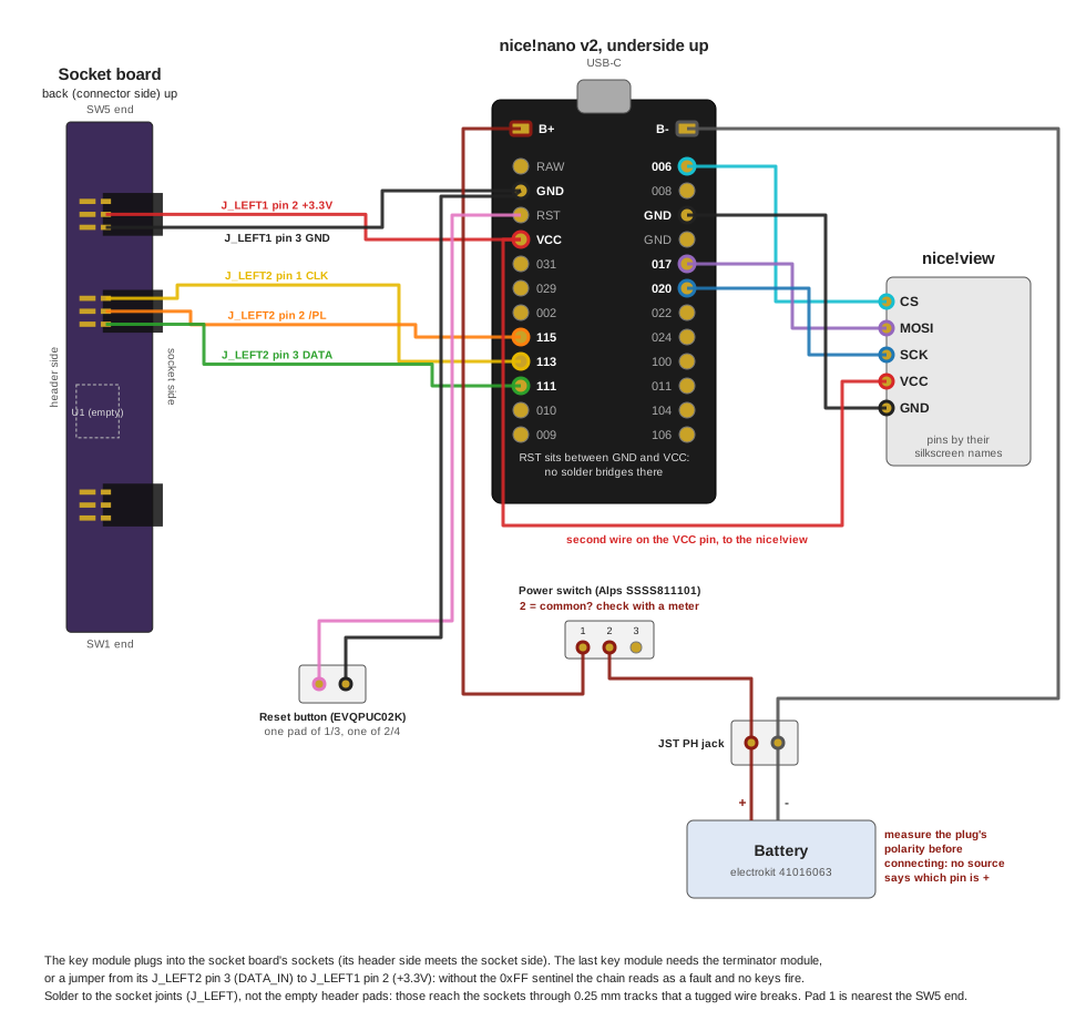
Wire the nice!nano, the nice!view and the socket board

#

Hover a signal to find it in every table.

J_LEFT1 (top)
1+5Vnot connected
2+3.3V→ VCC
3GND→ GND
J_LEFT2 (middle)
1CLK→ D15
2/PL→ D18
3DATA→ D14
J_LEFT3 (bottom)
1LEDnot connected
2SDAnot connected
3SCLnot connected
Signalnice!nanonRF52840Socket board
+3.3VVCCswitched by P0.13J_LEFT1 pin 2
GNDGNDJ_LEFT1 pin 3
CLKD15P1.13, SPIM1 SCKJ_LEFT2 pin 1
/PLD18P1.15J_LEFT2 pin 2
DATAD14P1.11, SPIM1 MISOJ_LEFT2 pin 3

nice!view

nice!viewnice!nanonRF52840
VCCVCCswitched by P0.13
GNDGND
SCKD3P0.20
MOSID2P0.17
CSD1P0.06

Solder the wires to the sockets' own joints (J_LEFT), not to the empty header pads (J_RIGHT) or U1's pads. Those reach the sockets through 0.25 mm tracks, and on the first socket board a wire tugging on a header pad broke the +3.3V and GND connections.

The reset button closes RST to GND. Mind the nano's RST pad: it sits between GND and VCC, so check for solder bridges there.

The wires from the socket board's pads and from the view cross the board's bay-side edge between the board-side tabs; route them there.

Wiring of the nice!nano, socket board, nice!view, battery, power switch and reset button
From docs/firmware.md. Click to enlarge.
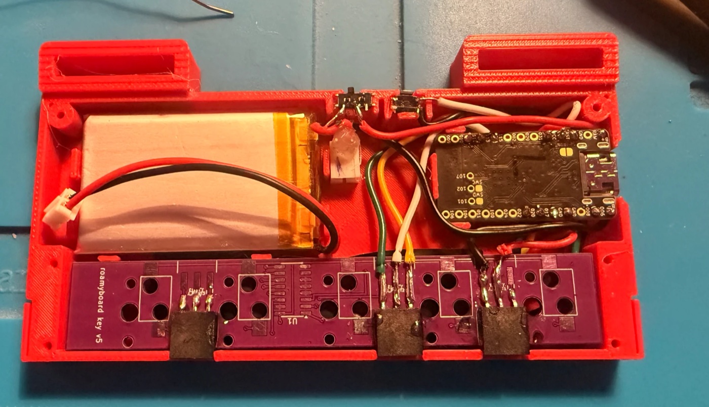
An open MCU module: battery, power switch, reset button, nice!nano and the socket board, with wires crossing the board edge to the sockets
A wired MCU module, open: the battery at the SW1 end, the power switch and reset button in their chambers, the nice!nano at the SW5 end, and the wires crossing the socket board's edge to the socket joints (2026-10-05).
Solder · check

Power: battery, jack and switch

#

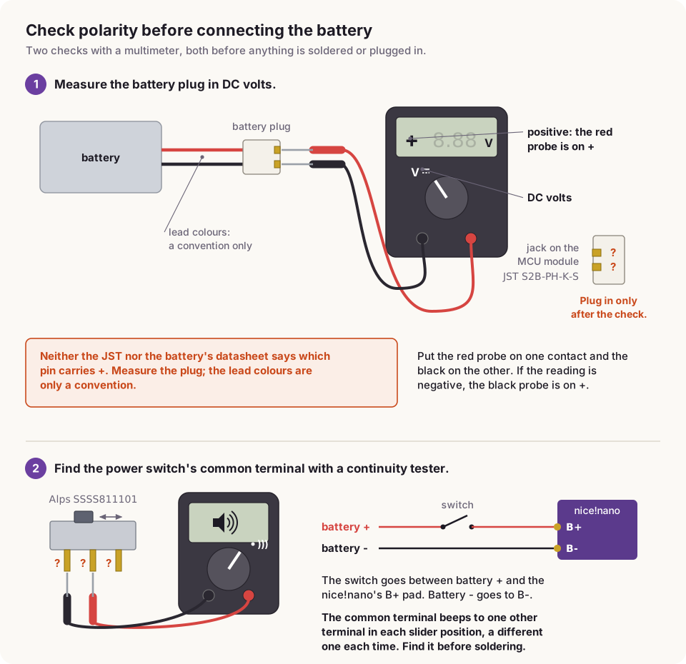
Battery + runs through the JST PH jack and the power switch to the nice!nano's B+ pad; battery − goes to B−.

  1. Measure the battery's plug with a meter in DC volts to find which contact is +. Neither the JST nor the electrokit datasheet says which jack pin the + lands on.
  2. Find the power switch's common terminal with a continuity tester; the Alps drawing was not checked for it.
  3. Wire the jack and the switch accordingly, and check the polarity at B+ and B− once more before the battery goes in.

With the switch off, USB still powers the nice!nano, but the battery does not charge. That was read from the nice!nano schematic and is untested.

Checking the battery plug's polarity and the switch's common terminal with a meter
Assemble

Assemble the MCU module

#

Everything that locates the parts sideways hangs from the plate, so the parts go into the upturned shell in this order, and the floor closes it:

  1. nice!view into its pocket under the window, header edge toward the nano's end. The wall at its flex end and the posts at its header end keep it in place.
  2. Socket board over it. The board-side tabs stop it sliding into the bay.
  3. Battery at the SW1 end, between its stops.
  4. nice!nano at the SW5 end: USB-C port into the end wall's slot, onto the post over the port and under the prop.
  5. Power switch and reset button into their chambers on the free face, slider and actuator outward.
  6. Battery jack onto its seat on the floor, mating face toward the battery.
  7. Floor on. Its tongue closes the USB slot under the port. Six M2 × 5 mm screws: four at the corners, as on a key module, and two in the bosses at the free face.

Step through it with the numbered buttons under the view.

8

Join a half

Start at the terminator module and work toward the MCU module: each module slides onto the headers of the one to its left.

Join

Slide-on

#
  1. Hold the new module's socket face to its neighbour's header face, tilted down by 8°, so that it moves along its own board plane.
  2. Push it straight on. The guide pins enter their holes first, 5.7 mm before the header pins reach the sockets, and line them up.
  3. The last 5.6 mm is the header pins going into the sockets. Over the last 2.3 mm the teeth ride the guide pins, and at the end they click into the notches.
  4. Repeat until the MCU module is on.

Drag Slide-on under the view.

Because the header is tilted, each module sits 1.1 mm lower at the seam than its neighbour. That is intended: it puts every module on the same arc.

Two joined key modules with purple keycaps held in a hand
The first two key modules joined: they mated, clicked and read as a chain (2026-09-26, an earlier case revision).
Join

Release and separation

#

There are two latches per seam, one at each column end.

  1. With the current tooth (45° catch face) the pair pulls apart by hand: pull the module off along its board plane.
  2. If a latch holds, lift its flap outward with a fingernail in the flap slot at its free edge, and pull.

The firmware counts key modules on every scan, so you can add or remove one while the keyboard runs. Keys stay quiet until the count has been stable for a few scans.

How stiff the flap is and how well the tooth holds in PLA versus PETG is not tested yet.

Slide-on, latching and release at one column end
Wear

Harness

#

The terminator module and the MCU module each have a lug at both column ends of their free face. Thread a strap through the four slots (up to 24 mm wide and 4 mm thick) and wear the half on your thigh. The lugs' undersides turn down by the joint angle to follow the leg.

The harness itself is not designed yet. From earlier prototypes: a good position is out toward the side of the thigh, leaning about 45°, at pocket height when standing and just above the knee when sitting, so it needs a way to move up and down the leg.

Photo wantedA finished half worn on the leg.
9

Flash and test

The Roamyboard runs ZMK with its own driver for the key modules' chain. Details in docs/firmware.md; the keys and layers are on the keyboard layout page.

Firmware

Get the firmware

#

GitHub Actions builds three UF2 files on every push that touches zmk/: download them from the latest run's artifacts in the Firmware workflow, or build locally with Docker (instructions).

FileForZMK Studio
roamyboardA unibody keyboard: one halfyes
roamyboard_leftThe left half of a split, which the computer connects toyes
roamyboard_rightThe right half of a splitno
Firmware

Flash

#
  1. Connect the MCU module over USB-C.
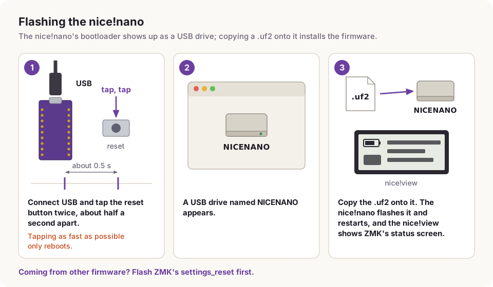
  2. Tap the reset button twice, about half a second apart. Tapping as fast as you can only reboots it.
  3. A drive named NICENANO appears. Copy the UF2 for this half onto it; the nice!nano flashes it and restarts.

If the nice!nano ran other firmware before, flash ZMK's settings_reset first, then the Roamyboard firmware. The first MCU module still carried Lily58 settings with behaviors that no longer existed. For a split, reset both halves if they do not find each other.

Only the first flash needs USB. Later updates can go over Bluetooth, from a Mac or a phone: hold L2 for the System layer and press OTA on the half (the keyboard layout shows where), then send the firmware as Updating over Bluetooth describes.

Double-tap reset, the NICENANO drive, copy the UF2
Test

First test

#
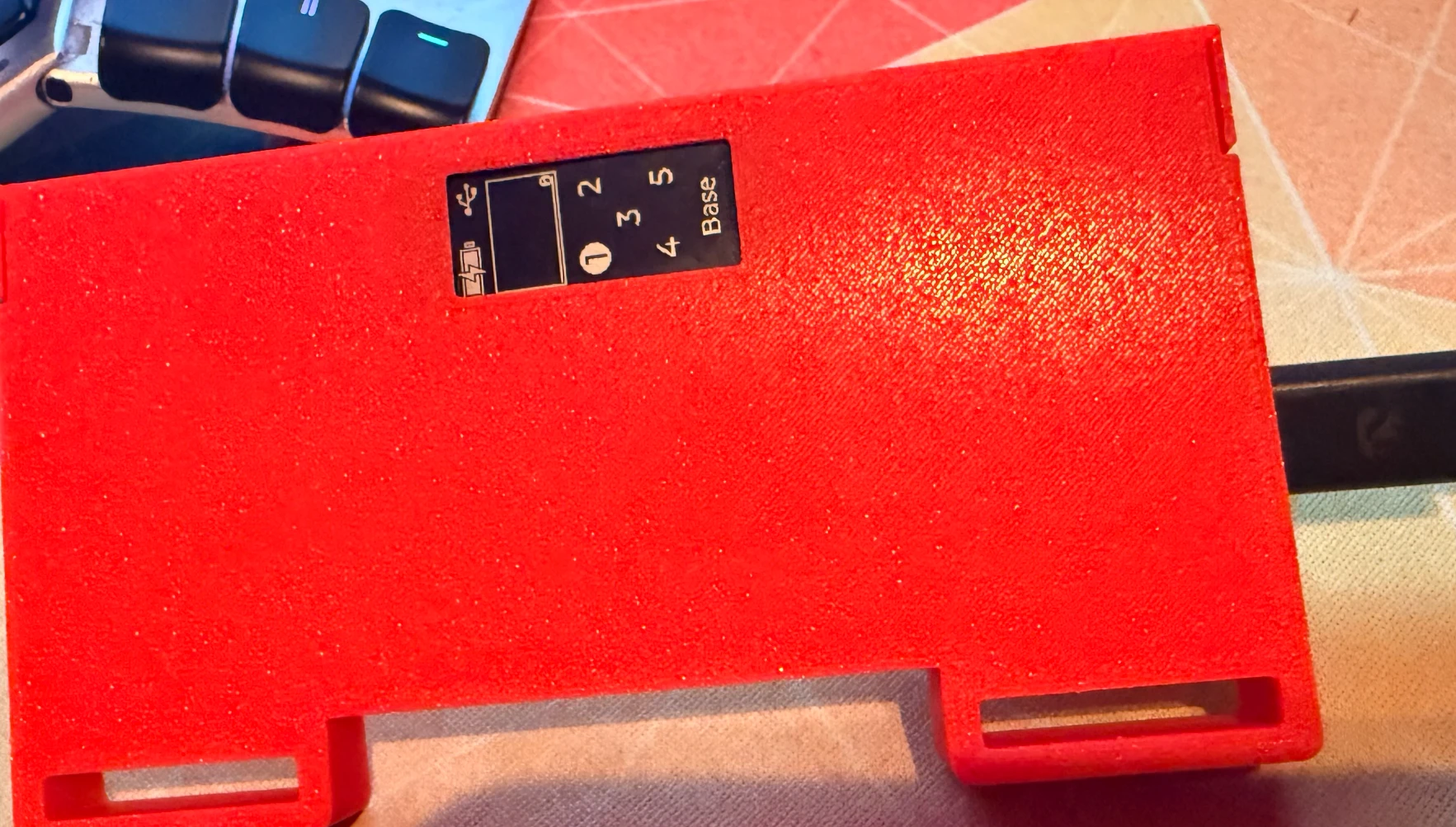
  • The nice!view shows the status screen: battery, connection, the key module count, the Bluetooth profiles and the layer, QWERTY.
  • With the terminator module on, the keys type the default layout, on the key modules nearest the middle of the keyboard.
  • Pair over Bluetooth: hold L2 (the left pinky's row 4 key) for the System layer, with four Bluetooth profiles, Bluetooth clear, the bootloader and reset.
  • Pull a key module off and put it back while it runs: the keys come back at their new keymap columns.

For logs, build with the zmk-usb-logging snippet and read the nice!nano's serial port: the driver reports the key module count and any fault with the raw bytes.

The MCU module's nice!view showing ZMK's status screen on first boot
First boot, 2026-09-27: ZMK's status screen through the MCU module's window.
10

Troubleshooting

What went wrong on the first builds, and what the firmware's symptoms mean.

Reference

Symptoms and causes

#
SymptomLikely causeFix
No keys at all; the log reports a faultNo sentinel: the terminator module is missing, DATA or /PL is broken, or there are more key modules than max-key-modules (32)Put the terminator module on; check DATA and /PL continuity through each joint
The count reads right at rest and drops to zero while a key is held; every byte goes to 0xFFThe 74HC165s have no supply and run on what leaks in through CLK and /PLCheck +3.3V and GND from the nice!nano to the socket board's socket joints, not to the J_RIGHT pads
Bootloader will not startThe reset taps are too fastTap twice about half a second apart
Strange behaviour right after flashingSettings left by earlier firmwareFlash settings_reset, then the Roamyboard firmware
Floor will not sit flatSolder or glue under the connector bodies; the tightest spot is 0.3 mm under the tilted headersTrim the fillet or bead

Not tested yet

  • Whether the 0.57 mm seat overhang prints clean, and how well the 0.25 mm seat holds a switch.
  • Flap stiffness and tooth hold in PLA versus PETG; the 0.1 mm guide clearance on other printers.
  • The MCU module r3 as a whole on the printer; charging with the power switch off.
  • One key module showed no GND continuity between its socket and header yet worked in either position, which a 74HC165 can also do on leaked ground. If a module acts up only in some positions, check its GND.
j k steps · x done